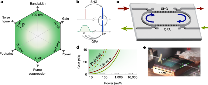
A research team demonstrated an integrated optical parametric amplifier on thin-film lithium niobate achieving over 17 dB gain with under 200 mW input—a roughly tenfold improvement in power efficiency versus prior chip-scale OPAs—using a second-harmonic-resonant design that yields ~95% pump conversion and nearly an order-of-magnitude effective pump-power enhancement. The device delivers flat, near-quantum-limited noise across ~110 nm bandwidth and is positioned to enable practical on‑chip broadband amplification for quantum and classical photonics; the work is supported by DARPA and is covered in part by a patent application, signaling potential commercialization pathways for lithium‑niobate photonics suppliers and integrators.
Market structure: Thin‑film lithium niobate (TFLN) OPAs that deliver >17 dB gain at <200 mW lower a key barrier for on‑chip amplification, directly benefiting TFLN foundries, photonic‑PIC integrators and wafer‑equipment suppliers (expect demand lift for AMAT/KLAC class tools). Incumbent EDFA/semiconductor amplifier revenue pools (vendors with large EDFA exposure and standalone SOA modules) face pricing pressure in mid/long haul and photonic sensor niches; network equipment vendors who adopt on‑chip gain can gain share in coherent pluggables and repeaterless links (positive for CIEN, LITE). Cross‑asset: modest positive for capex‑sensitive semicap equities and cyclicals; limited near‑term FX/bond impact, but potential long‑duration revenue re‑phasing could lower telecom capex cyclicality over 2–5 years and tighten credit spreads for growth names in the space.
Risk assessment: Tail risks include failure to scale packaging (facet/coupling loss >1 dB), IP blocking from patentees (authors have pending IP), or alternative tech (SiN/Si) improving faster; any of these could make projected TAM capture drop >50% over 2 years. Time horizons: immediate (days) — no material market move; short (3–9 months) — partnership/MOU and foundry capacity signals; long (12–36 months) — product integrations and revenue inflection if coupling losses <1 dB and manufacturable yields >70%. Hidden dependencies: system redesign cost, standards for pluggables, and supply constraints for high‑quality LN wafers; catalysts to watch are DARPA/NTT partnership announcements, foundry capacity expansions, and first carrier field trials.
Trade implications: Tactical: establish a modest 1.5–2.0% long in Ciena (CIEN) as a play on coherent pluggables adoption over 12 months (trim if stock +30% or if CIEN reports no OEM engagement in 90 days). Pair trade: long CIEN (2%) / short Infinera (INFN) (1.5%) over 6–12 months to capture relative wins from architecture shifts; rebalance if spread moves >25%. Express options: buy 9–12 month AMAT call spreads (size ~1% notional, delta ~0.30) to play increased photonics fab capex; reduce or avoid incremental exposure to IPG Photonics (IPGP) by 1–2% pending customer revenue hits in amplifier segments.
Contrarian angles: The market may under‑price manufacturing and packaging bottlenecks — revenue disruption is unlikely to be front‑loaded; adoption will be choppy and concentrated in high‑value sensing/coherent markets first. Analogous precedent: silicon photonics took 5–7 years from lab demos to material revenue; expect similar multi‑year cadence, not immediate disruption. Watch for consolidation: larger optical vendors may acquire TFLN foundries — such M&A would be a positive catalyst for the long‑positions and should trigger a size+ event if announced.
AI-powered research, real-time alerts, and portfolio analytics for institutional investors.
Request DemoOverall Sentiment
moderately positive
Sentiment Score
0.48
