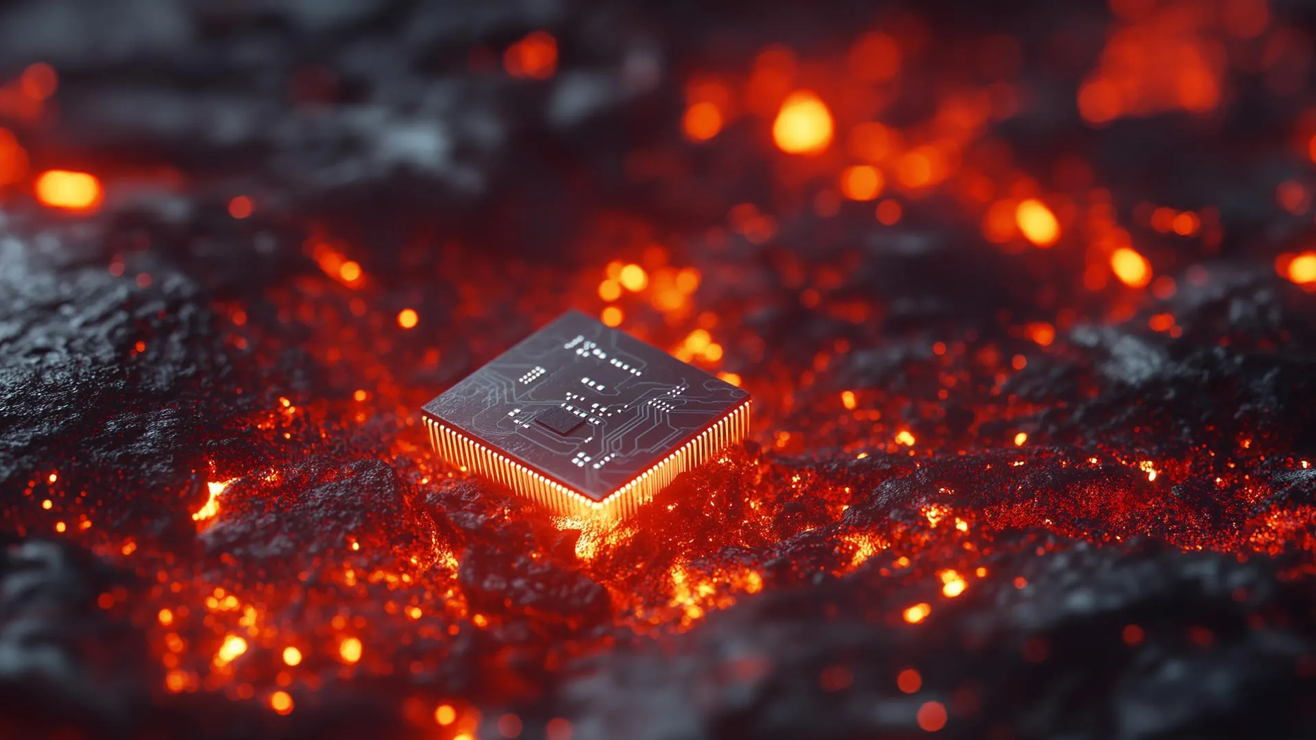
Researchers at USC demonstrated a memristor that operates at 700°C (1300°F), retaining data >50 hours and surviving >1 billion switching cycles while operating at 1.5V and tens of nanoseconds. Built from tungsten/hafnium oxide/graphene, the device enables high-temperature in-memory AI compute and targets applications in space (e.g., Venus), geothermal, nuclear/fusion, and industrial sensing. The team co-founded TetraMem to commercialize room-temperature chips; scaling to production requires high-temperature logic development and manufacturing scale-up (graphene wafer efforts at TSMC/Samsung noted). The work is backed by the CONCRETE Center and Air Force collaborators, implying strategic and defense relevance.
The research creates a new vector of competition beyond logic-node scaling: process-material differentiation. Foundries and equipment OEMs that control wafer-scale integration of novel 2D interfaces and refractory-metal stacks will capture outsized margin expansion versus pure-play IDMs that lack advanced back-end process toolsets. Expect supplier leverage (deposition, etch, metrology) to translate into multi-year incremental CapEx cycles—if graphene/2D stacking becomes a design rule, tool spend per wafer could re-rate those vendors’ TAMs by a low-double-digit percentage within 3 years. Second-order supply risks are underappreciated: specialty refractory metals and high-purity hafnium streams are concentrated and tied to niche processing (zirconium/hafnium separation, tungsten refining). Bottlenecks here would create profitable arbitrage for upstream miners and chemical processors but would also invite vertical integration or long-term offtake deals from large fabs. Sovereign-security considerations (defense/space demand) can accelerate procurement and create preferential sourcing corridors that benefit contractors with existing government relationships. Execution risk sits squarely on manufacturability, not physics. The milestone cadence to watch is wafer-scale yield and BEOL compatibility—until both are demonstrated at pilot scale, revenue is optional; the most likely timeline for commercial foundry adoption is 24–48 months for pilot lines and 3–6 years for volume production. IP and standards fights (university spinouts vs. industry incumbents) present a medium-term catalyst or constraint depending on licensing outcomes and who secures early foundry partnerships. The market’s narrative will bifurcate: near-term hype around “revolutionary” compute vs. sober engineering reality of system-level integration (logic, interconnect, packaging). We should therefore overweight firms that sell into process integration (equipment, metrology, defense primes that can finance early pilots) and underweight speculative pure-play material explorers until demonstrated supply contracts or wafer-level yields exist.
AI-powered research, real-time alerts, and portfolio analytics for institutional investors.
Request DemoOverall Sentiment
strongly positive
Sentiment Score
0.70
Ticker Sentiment