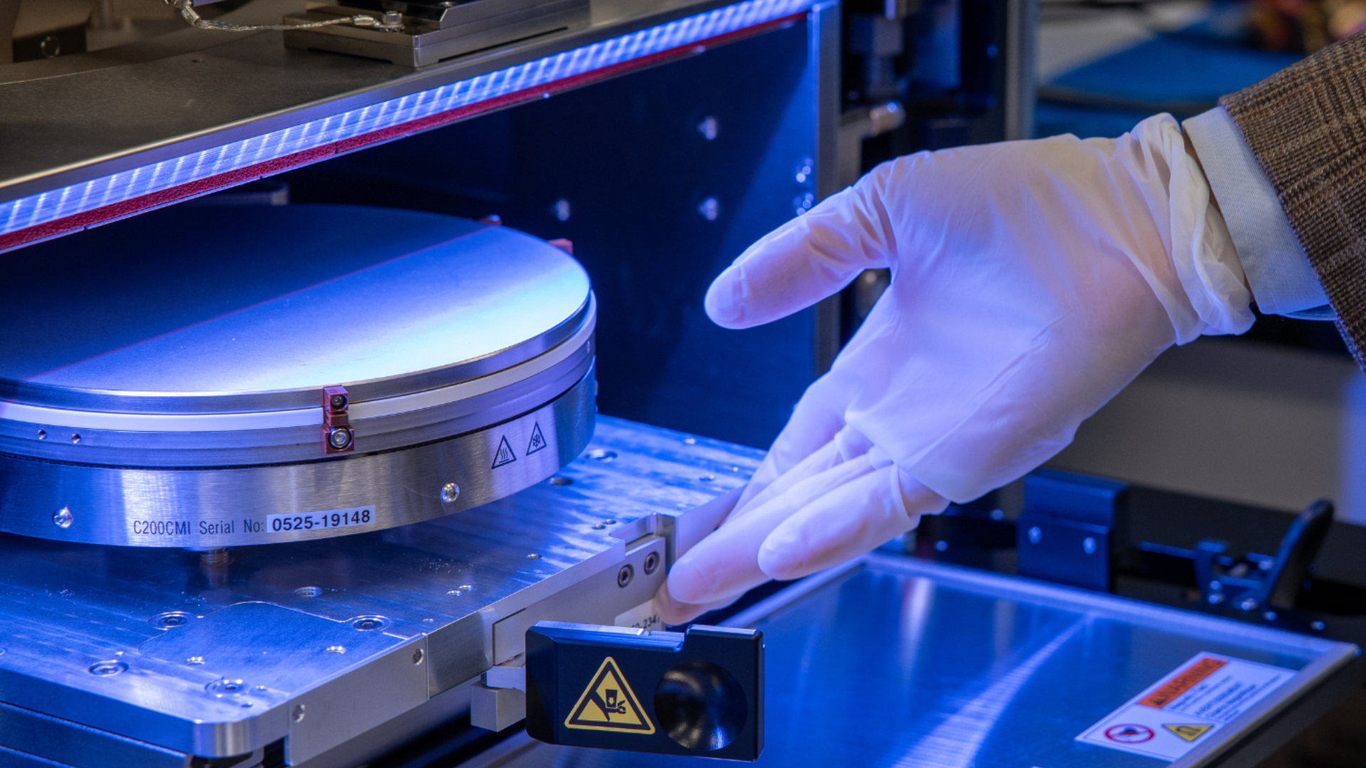
A multi-university team and SkyWater Technology fabricated what they say is the first monolithic 3D integrated circuit in a U.S. commercial foundry, stacking CMOS logic, resistive RAM and carbon‑nanotube FETs on a 200mm line using a 90–130nm process with a ~415°C thermal budget to create dense vertical interconnects. Early hardware tests showed roughly 4x throughput versus a comparable 2D implementation and simulations of taller stacks delivered up to 12x speedups on AI-style workloads (including LLaMA-derived models), with the group projecting eventual 100x–1,000x improvements in energy‑delay product as vertical integration scales. By demonstrating the approach in a production fab (presented at IEDM 2025), the work signals that monolithic 3D integration could be manufacturable domestically and offers an alternative path to performance and efficiency gains for AI accelerators and memory-compute architectures beyond continued transistor shrinkage.
A multi‑university team and SkyWater Technology reported the first monolithic 3D integrated circuit fabricated in a U.S. commercial foundry, stacking CMOS logic, resistive RAM and carbon‑nanotube FETs on a 200mm line using a mature 90–130nm process under a ~415°C thermal budget. Devices were built sequentially on the same wafer to create dense vertical interconnects that shorten memory‑compute paths relative to conventional 2D dies, and SkyWater presented the work at IEDM 2025 to demonstrate transfer into domestic manufacturing flows.
Measured hardware tests on the prototype showed roughly 4× throughput improvement versus a comparable 2D implementation at similar latency and footprint, while simulations of taller stacks showed up to 12× speedups on AI‑style workloads including LLaMA‑derived models; the team projects potential 100×–1,000× energy‑delay gains with continued vertical scaling. The result signals an alternative path to performance gains for AI accelerators and memory‑compute integration that emphasizes architecture scaling over transistor shrink.
Near‑term constraints include the low‑temperature process that limits aggressive node shrink and attendant compute density, the prototype's fabrication on mature nodes (90–130nm) which leaves cost and competitiveness unanswered, and parallel historical cautionary examples (chalcogenide/Optane) that underscore commercialization risk. Market adoption depends on yield metrics, scaling roadmaps and customer qualification beyond a single proof‑of‑concept in a commercial fab.
AI-powered research, real-time alerts, and portfolio analytics for institutional investors.
Request DemoOverall Sentiment
moderately positive
Sentiment Score
0.50
Ticker Sentiment
