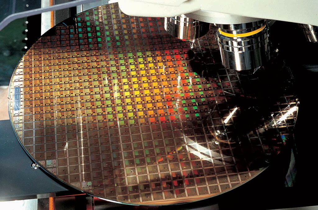
Researchers at MIT, with collaborators at the University of Waterloo and Samsung, demonstrated a backend fabrication approach that adds an extra layer of microscopic transistors to finished dies by depositing a low-temperature, 2 nm amorphous indium oxide film (and using ferroelectric hafnium‑zirconium oxide to form memory cells), enabling higher on‑die transistor density without thermally damaging front‑end structures. The technique effectively creates an additional transistor plane on the back end, offering a potential cost‑effective alternative to extreme node scaling, but remains at an early research stage without yet producing production‑ready circuits. If scalable and combined with existing 3D stacking methods, the approach could materially extend transistor density gains and alter the economics of advanced logic and memory roadmaps.
Researchers at MIT with collaborators at the University of Waterloo and Samsung Electronics demonstrated a backend fabrication approach that deposits a very thin (2 nm) amorphous indium oxide layer on finished dies to form an additional transistor plane and used ferroelectric hafnium-zirconium oxide to create memory cells. The team claims this low-temperature process avoids thermal damage to the front-end transistors and effectively increases on-die transistor density without moving to smaller, more expensive process nodes.
This technique represents a potential alternative or complement to traditional node scaling and chip stacking: if it can be integrated with existing architectures it could materially change density gains and the economics of future logic and memory roadmaps. The article explicitly notes the work is still early-stage and has not yet delivered production-ready circuits, so technical validation (functional circuits, yield, reliability) remains outstanding.
Market signals attached to the report are mildly positive (sentiment_score 0.3, market_impact_score 0.25) and the only ticker highlighted (AMD) is not a direct subject of the research (per-ticker sentiment 0.0), implying limited immediate market impact. Key risks are process integration, scaling to high-volume manufacturing, yield and reliability under operating conditions, and the timeline for foundry adoption, which will determine any substantive commercial or valuation effects.
AI-powered research, real-time alerts, and portfolio analytics for institutional investors.
Request DemoOverall Sentiment
mildly positive
Sentiment Score
0.30
Ticker Sentiment
