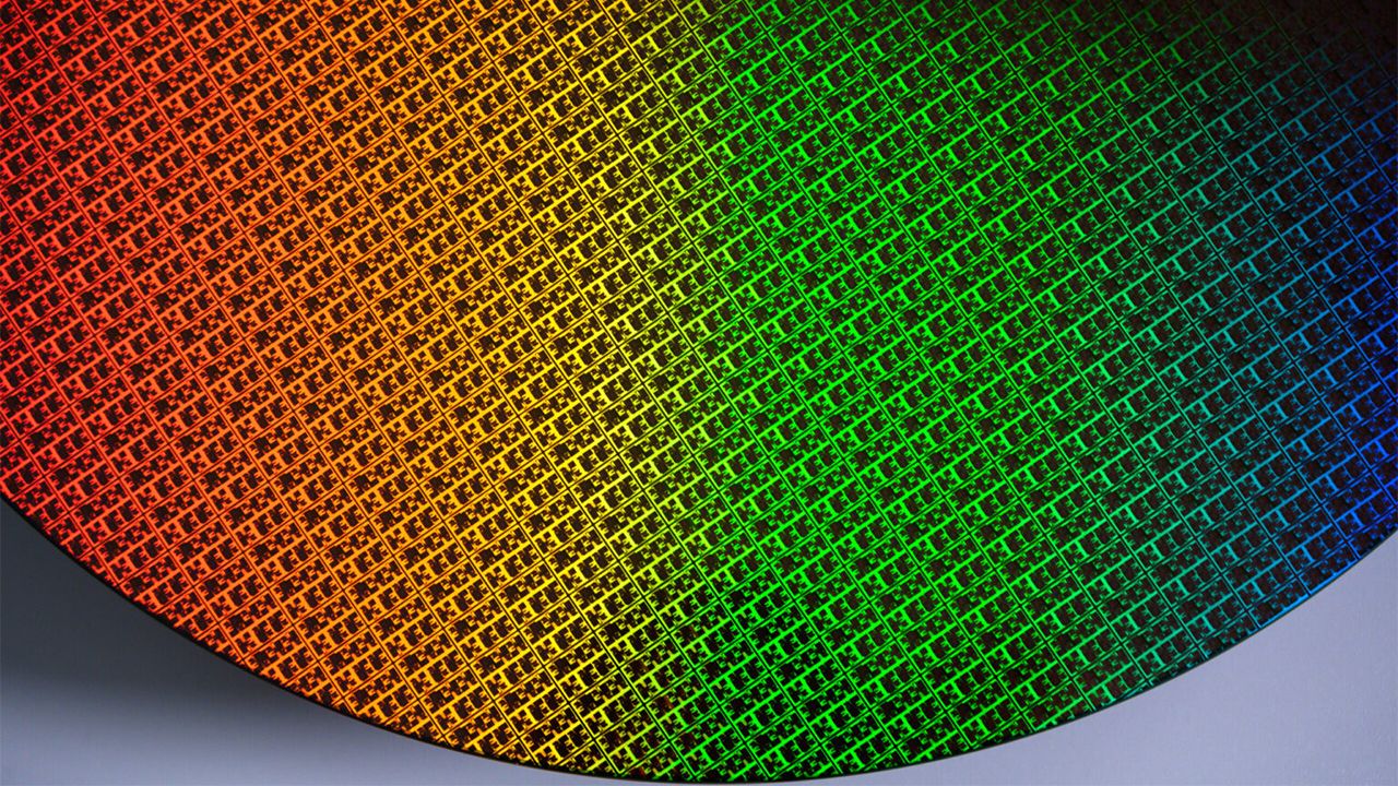
Researchers at Fudan University have achieved a significant breakthrough by successfully integrating a fully functional 2D NOR flash memory array, made from atomic-thin molybdenum disulfide, directly onto a conventional 0.13-micrometer CMOS silicon chip. This hybrid design, utilizing their ATOM2CHIP process, demonstrates high yield (94.34%), 5 MHz operational speeds, and ultra-low energy consumption (0.644 pJ/bit), along with robust data retention and endurance. This development marks a critical step towards commercializing 2D electronics, promising drastic power reduction and increased density for future processors and AI, potentially extending Moore's Law, despite mass production still being years off.
Researchers at Fudan University have achieved a significant milestone by successfully integrating a functional 2D NOR flash memory array, composed of atomic-thin molybdenum disulfide, directly onto a conventional 0.13-micrometer CMOS silicon chip. This ATOM2CHIP process yielded an impressive 94.34% from full-chip testing, rivaling commercial silicon production. The resulting hybrid memory demonstrates ultra-low energy consumption of just 0.644 picojoules per bit and operational speeds up to five megahertz.
The team overcame critical challenges, including silicon surface roughness, through a conformal adhesion process and a 2D-friendly packaging system. This innovation ensures the integrity of the atomic-thin layers and protects against environmental damage. The memory also exhibits robust performance with fast 20-nanosecond programming/erasing, ten-year data retention, and endurance exceeding 100,000 write cycles.
This development holds substantial implications for the semiconductor industry, particularly for next-generation processors and AI accelerators. The hybrid architecture promises drastic reductions in power consumption and increased density, potentially extending Moore's Law at the atomic limit. While mass production remains years away, this breakthrough represents the closest 2D materials have come to commercial viability, signaling a potential paradigm shift in chip manufacturing.
AI-powered research, real-time alerts, and portfolio analytics for institutional investors.
Request DemoOverall Sentiment
extremely positive
Sentiment Score
0.85
Ticker Sentiment
