
Hanyang University Researchers Gain Control Over Where Semiconductor Crystals First Form
Source: PR Newswire
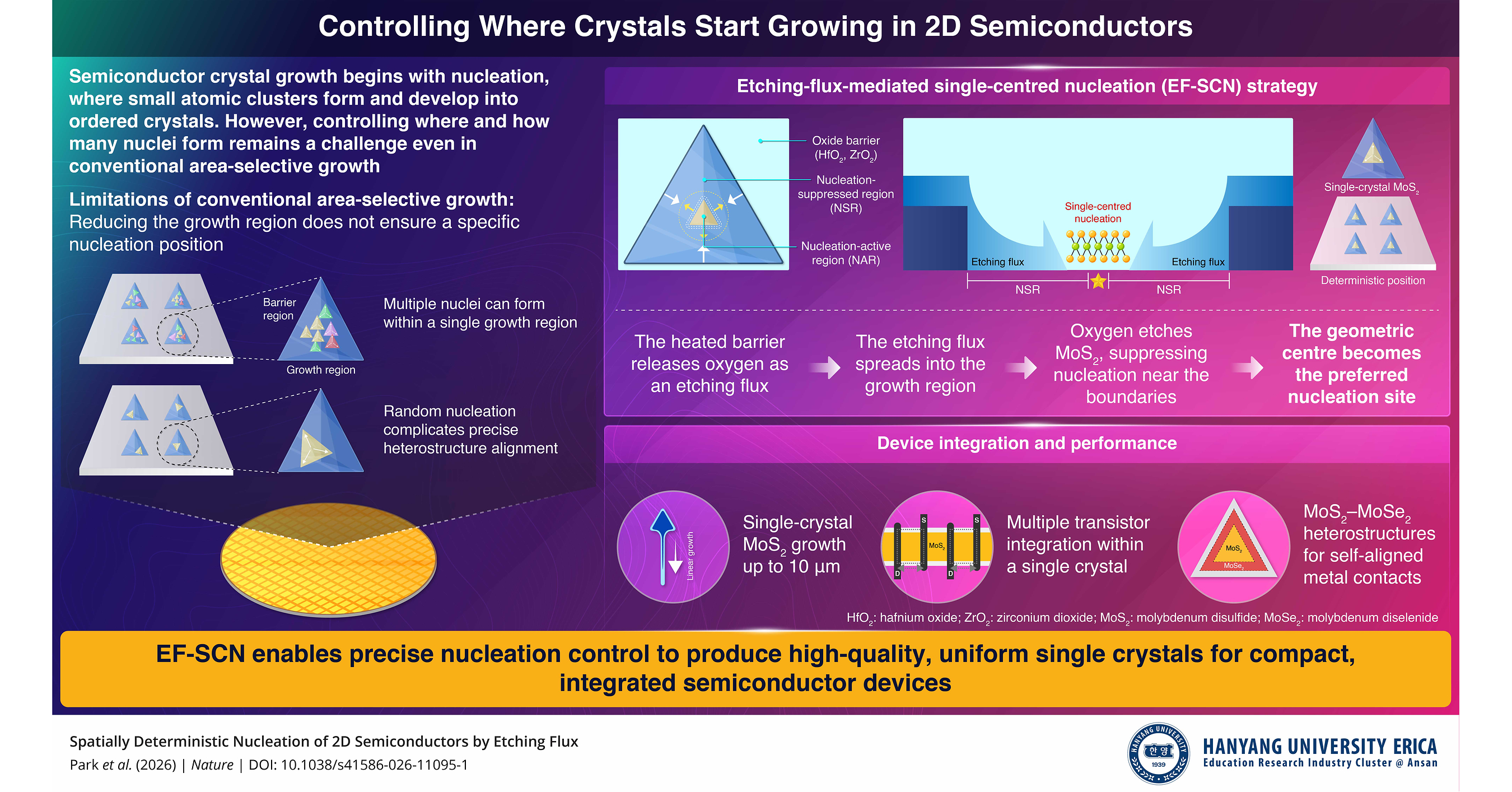
Hanyang University researchers reported over 99% single-crystal growth across 400 sites on a 2-centimetre substrate using a method that controls where MoS₂ crystals nucleate. The process produced crystals about 8 micrometres across, including growth at temperatures as low as 430°C with an alternative barrier; test transistors achieved field-effect mobility up to 117 cm² V⁻¹ s⁻¹. The results demonstrate potential for more consistent semiconductor device integration, but the article reports research findings rather than commercial deployment.
Analysis
The investable signal is process control, not near-term MoS₂ revenue. Deterministic nucleation could eventually reduce defect and placement variability in 2D-semiconductor devices, but the reported site yield on a 2-centimetre substrate does not establish wafer-scale uniformity, repeatable device performance, or compatibility with existing CMOS flows. The key translation hurdles are defectivity across larger substrates, contact resistance and stability, throughput, and integration within thermal and contamination budgets. The 430°C variant improves the integration case versus the higher-temperature route, but does not resolve those other constraints.
Near term, this is unlikely to change semiconductor earnings or justify repricing equipment/materials suppliers; the work is academic, with no disclosed commercialization, customer qualification, or manufacturing economics. Over 1–3 months, watch for independent replication and evidence of larger-area growth and functional circuits. Over 6–18 months, a credible path to pilot-line integration could benefit the broader 2D-materials process ecosystem, while incumbent silicon process flows remain the default absent compelling performance and cost advantages.
Contrarian angle: the impressive site-level yield and best-device mobility can invite extrapolation to manufacturing readiness. They are not substitutes for wafer-scale yield, distribution of device metrics, lifetime, or cost-per-good-device data. No company-specific trade is supported by this announcement.
AllMind Terminal
AI-powered research, real-time alerts, and portfolio analytics for institutional investors.
Request TrialMarket Sentiment
Overall Sentiment
mildly positive
Sentiment Score
0.30
Key Decisions for Investors
- No immediate position: do not chase 2D-semiconductor or semiconductor-equipment exposure on this paper alone.
- Set a 1–3 month watch for independent replication, substrate-area scaling, device-to-device performance distributions, and evidence of pilot-line or commercial partnerships.
- Reassess the 6–18 month opportunity only if larger-scale demonstrations show repeatable electrical performance and integration-compatible process conditions; that would support targeted research into 2D-material process and equipment beneficiaries.
- Falsify the prospective adoption thesis if scaling materially degrades single-crystal yield or device consistency, or if contact, reliability, throughput, or thermal-budget constraints prevent integration.
More News
- Tech stock rout, driven by US AI fears, continues in Asian trading
- Asian Markets Tally Losses From Worsening Global Rout
- AI’s Grip on Financial Markets Was Never Clearer on the Way Down
- Elon Musk once said the Cybertruck would be Tesla’s ‘best product ever.’ Now he’s winding down production
- OpenAI valued at $1.25 trillion, as rival Anthropic nears its IPO
- AI Party isn't Ending Because Of The Blue Wave Says Ives